
India's Semiconductor Ecosystem: Inside the Mega Fabs in Gujarat and Assam

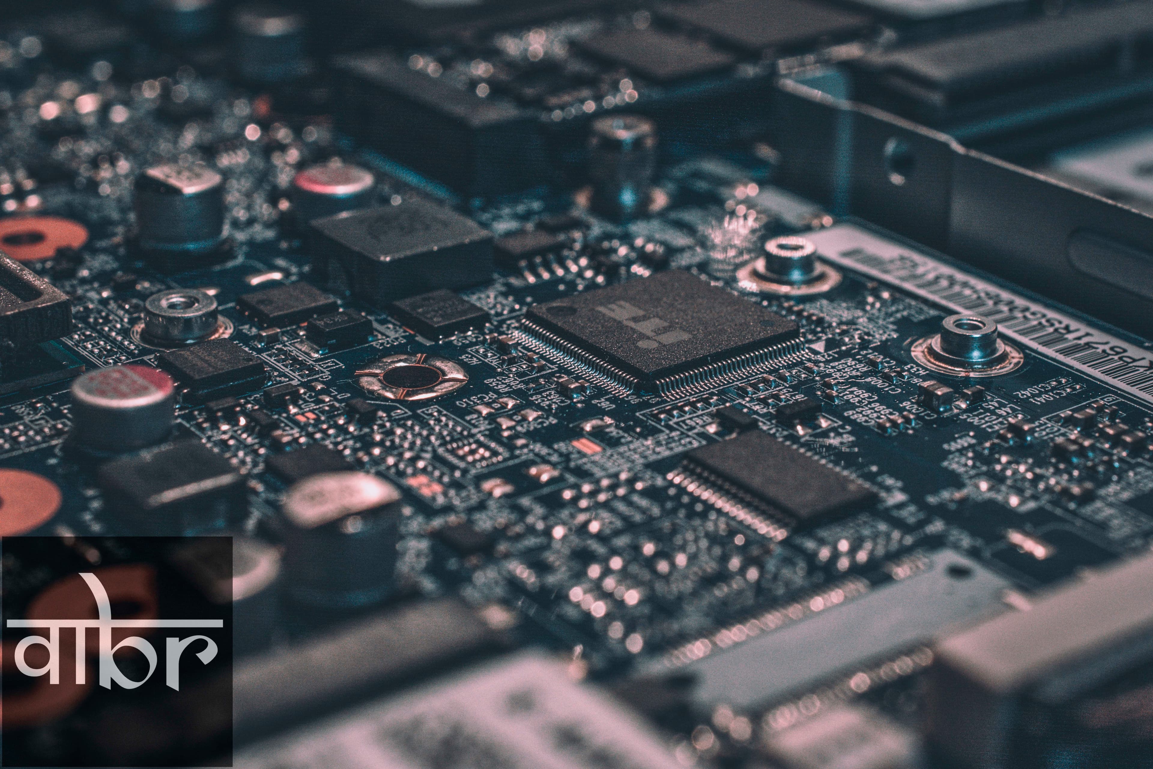
For decades, India held an undisputed global reputation in chip design, housing research labs for Qualcomm, Intel, Nvidia, and Texas Instruments. Yet despite employing roughly 20% of the world’s integrated circuit design engineers, the country lacked a single commercial silicon foundry capable of manufacturing those designs domestically. Every wafer designed in Bengaluru or Hyderabad had to be sent to East Asia—predominantly Taiwan, South Korea, or mainland China—for fabrication, assembly, and packaging.
The vulnerabilities of that structural imbalance were laid bare during the post-pandemic supply chain shocks and escalating geopolitical tensions across the Taiwan Strait. Through the India Semiconductor Mission (ISM) and its foundational fiscal support framework, that status quo is undergoing a decisive shift. With mega-scale fabrication plants and high-volume packaging hubs underway across Gujarat and Assam, India is aggressively transitioning from a software-centric technology hub into a hardware-independent manufacturing economy.
The Anchor Projects: Dholera, Sanand, and Morigaon
The central pillar of India’s semiconductor strategy rests on a bifurcated approach: commercial silicon fabrication (front-end) and advanced packaging (back-end). Developing both simultaneously prevents the bottlenecks that emerge when wafers must be shipped overseas merely for slicing, wire-bonding, and quality testing.
1. Tata Electronics & PSMC Commercial Fab (Dholera, Gujarat)
Located within the Dholera Special Investment Region (SIR), this greenfield mega-fab represents a committed investment of approximately ₹91,000 crore ($11 billion). Developed in partnership with Taiwan's Powerchip Semiconductor Manufacturing Corporation (PSMC), the Dholera plant is designed to reach an operational volume of 50,000 wafer starts per month.
Critically, the facility is not targeting sub-3nm bleeding-edge smartphone chips. Instead, it focuses on mature, high-volume process nodes: 28nm, 40nm, 55nm, and 90nm. In the automotive, industrial control, power management, and IoT sectors, these legacy and mature nodes represent the vast majority of real-world volume demand.
2. Assembly, Testing, Marking, and Packaging Hubs (Sanand, Gujarat)
Sanand has rapidly consolidated into a premier packaging and testing cluster, hosting multiple strategic projects:
- Micron Technology: A $2.75 billion phased facility focusing on dynamic random-access memory (DRAM) and NAND flash memory assembly and test modules.
- CG Semi (CG Power, Renesas, and Stars Microelectronics): A specialized packaging unit delivering chips tailored to industrial power conversion, telecom infrastructure, and electric vehicle drives.
- Kaynes Semicon: A high-throughput OSAT facility engineered to package millions of microchips daily for consumer smart electronics and smart energy meters.
3. Tata Semiconductor Assembly and Test (Morigaon, Assam)
In a major geographical diversification for Indian heavy technology, Tata Electronics established a ₹27,000 crore ($3.2 billion) outsourced semiconductor assembly and test (OSAT) facility in Morigaon, Assam. Engineered for an operational capacity of 48 million chips daily, the Morigaon site focuses on advanced packaging techniques—including wire-bond, flip-chip, and system-in-package (SiP) configurations. The plant directly connects northeastern India into the high-tech electronics value chain.
Project | Location | Key Stakeholders / Partners | Focus Area | Capacity Target |
|---|---|---|---|---|
Dholera Fab | Dholera, Gujarat | Tata Electronics, PSMC (Taiwan) | 28nm, 40nm, 90nm Logic & Power | 50,000 wafer starts/month |
Micron ATMP | Sanand, Gujarat | Micron Technology | Memory (DRAM, NAND packaging) | High-volume export & domestic supply |
CG Semi OSAT | Sanand, Gujarat | CG Power, Renesas (Japan), Stars Micro | Power management, MCUs, EV controllers | 15 million units/day |
Tata OSAT | Morigaon, Assam | Tata Electronics | Advanced flip-chip, ISIP, wire-bond | 48 million units/day |

Why ATMP and OSAT Precede Bleeding-Edge Silicon
A recurring critique from casual industry observers is that India’s first wave leans heavily into packaging (ATMP/OSAT) and mature node sizes rather than 2nm or 3nm lithography. From an operational and economic perspective, this sequencing is deliberate.
First, leading-edge foundries require capital outlays upwards of $20 billion per facility and rely on ultra-complex Extreme Ultraviolet (EUV) lithography systems with years-long backorders. Starting at mature nodes (28nm to 90nm) allows domestic engineers and cleanroom technicians to master process yields, contamination controls, and ultra-pure chemical handling without crippling financial overhead.
Second, the physics of semiconductor scaling has made advanced packaging just as critical as raw transistor shrinking. Through techniques like chiplet integration and 2.5D/3D stacking, modern devices achieve dramatic performance gains by wiring separate dies together on a common substrate. By anchoring world-class packaging units in Sanand and Morigaon, India secures a vital slice of modern computing architecture from day one.
Overcoming the Infrastructure Hurdle
Building out a semiconductor foundry goes far beyond erecting a sterile cleanroom facility. Fabs require a continuous, fault-free operating environment where even a fractional-second power flicker or chemical impurity can ruin an entire production cycle.
- Ultra-Pure Water (UPW): Processing a single 300mm wafer requires thousands of gallons of water purified to parts-per-billion standards. Facilities in Dholera and Sanand depend on dedicated multi-stage filtration pipelines, desalination access, and extensive water-recycling loops that reclaim up to 90% of process water.
- Uninterruptible Industrial Power: Foundries cannot tolerate voltage drops. Dedicated dual-grid substations and industrial-scale battery and gas-turbine backup systems have been prioritized around the manufacturing clusters.
- Specialty Gases and Sub-Suppliers: Silicon wafers must be treated with ultra-high-purity gases (silane, nitrogen, argon) and wet chemicals. The entry of global chemical and gas distributors into India's domestic supply pipeline is vital to avoid reliance on airfreighted raw materials.
What This Means for Domestic Hardware Independence
India’s heavy dependence on imported electronics has historically presented both economic and defense liabilities. By establishing operational silicon fabs and packaging hubs domestically, the country captures three strategic dividends:
Strategic Defense and Critical Infrastructure
National defense grids, smart electrical switches, space systems, and radar installations cannot run on untrusted components vulnerable to backdoors or external embargoes. Having sovereign control over fabrication runs guarantees trusted hardware integrity for sovereign security assets.
Automotive and Clean Mobility Resilience
Modern electric vehicles and hybrids consume hundreds of semiconductor units per chassis, ranging from battery management systems (BMS) to motor controllers. India's burgeoning automotive corridor now gains a localized supply buffer against geopolitical disruptions.
Completing the "Design-to-Device" Loop
With thousands of local engineers already drafting chip designs at domestic design centers, having physical foundries in Gujarat and packaging hubs in Assam closes the feedback loop. Prototyping cycles that once required months of overseas turnaround can eventually occur within domestic borders, spurring an organic ecosystem of Indian fabless startups.
Frequently Asked Questions
When will commercial chips roll out from these facilities?
The first commercial packaging outputs from Sanand have entered testing and volume delivery phases, with Tata Electronics' Dholera fabrication unit scheduled to initiate early trial runs and commercial production ramp-ups across 2026.
Why isn't India building 3nm or 5nm processor fabs?
Processors below 7nm serve high-performance smartphones and AI accelerators, requiring multi-billion-dollar EUV equipment and decades of proprietary institutional knowledge. Mature nodes (28nm to 90nm) command the highest commercial market share globally across automotive, defense, home appliances, and telecom equipment.
What is the difference between an OSAT/ATMP facility and a fabrication unit?
A semiconductor fabrication unit (fab) creates the microscopic circuits and transistors directly onto a raw, polished silicon wafer. An ATMP or OSAT facility takes that finished wafer, dices it into individual dies, tests them, bonds them into protective packages, and attaches electrical pins so they can be mounted onto printed circuit boards.
India’s multi-pronged expansion across Dholera, Sanand, and Morigaon proves that the nation is no longer content with simply designing silicon for international conglomerates. By laying the heavy, capital-intensive groundwork across both fabrication and packaging, India is building the structural foundation required for long-term technological self-reliance.
Varta Brief Editorial Desk
• Newsroom StaffDedicated to objective, deep, and fact-verified reporting across technology, science, world affairs, and modern markets.
Follow Varta Brief on Google
Add Varta Brief as a preferred source to see our verified stories and daily briefings in Google Top Stories and Discover.
Found this briefing insightful?
Share it with your colleagues and community.
